Semiconductor freight: logistics for the chip supply chain
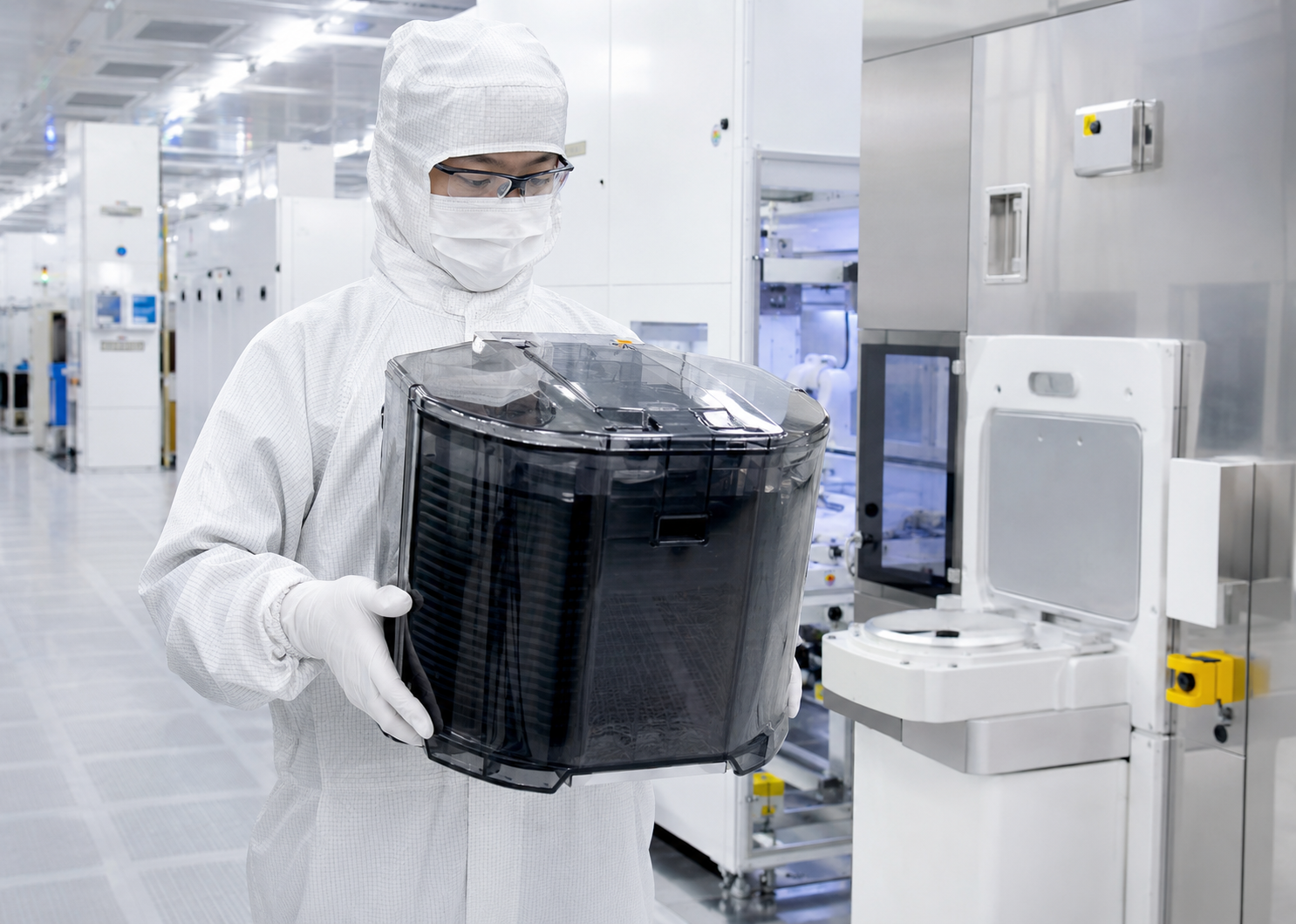
The global semiconductor supply chain is one of the most complex and time-sensitive logistics environments in manufacturing. A single chip fabrication facility can represent $20 billion in capital investment and run continuous production cycles where unplanned downtime is measured in millions of dollars per hour. The equipment, materials, and components that keep those facilities running have to move with a speed and reliability that most standard freight providers cannot accommodate.
Expedited freight for semiconductor and chip manufacturing covers a range of scenarios — from emergency tool parts and critical process chemicals to finished wafer shipments with strict environmental handling requirements. This guide covers what semiconductor freight actually involves, what makes it different from standard industrial logistics, and what procurement and supply chain teams should look for in an expedited freight broker.
What semiconductor freight involves
Fabrication equipment parts — line-critical and line-down
Semiconductor fabrication equipment — lithography systems, etch tools, chemical vapour deposition reactors, ion implanters — operates continuously and at extreme precision. When a component fails, the production line stops. These are not situations where waiting 24 hours for next-day delivery is acceptable — the cost of a single hour of fab downtime at a leading-edge facility typically exceeds the cost of the most aggressive expedited freight option available.
The parts involved range from common wear items that a facility might keep in local stock to highly specialised optical or mechanical components that come from a single manufacturer, often overseas, and require careful coordination across multiple carriers and customs regimes to move quickly.
Process chemicals and specialty gases
Semiconductor fabrication consumes substantial volumes of high-purity process chemicals and specialty gases — etchants, photoresists, dopants, cleaning agents, and process gases including some that are both toxic and extremely reactive. These materials require hazmat-certified carriers, specific packaging that meets DOT and IATA dangerous goods regulations, and handling procedures that prevent contamination or exposure. An expedited freight broker moving semiconductor chemicals needs carriers with the appropriate hazmat authority — this is not a capability that can be improvised when an urgent shipment arises.
Wafers and finished product
Processed semiconductor wafers and finished die represent enormous value per unit volume — a single wafer can contain thousands of chips worth hundreds of dollars each. Wafer shipments require vibration-controlled transport, electrostatic discharge (ESD) protective packaging, controlled temperature and humidity environments, and in some cases cleanroom compatibility at the origin and destination. The carrier handling a wafer shipment needs to understand these requirements, not learn them on the day of pickup.
Photomasks and reticles
Photomasks and reticles — the precision optical elements used in lithography to pattern circuit features onto wafers — are irreplaceable, extremely valuable, and extremely fragile. A damaged reticle can halt production for weeks while a replacement is manufactured. Transport requires purpose-built protective cases, vibration isolation, and very careful handling procedures. This is not a shipment type that should go through standard freight networks.
Tooling qualification samples
When new equipment is being qualified or when a process is being transferred to a different facility, qualification wafers and process samples move between sites on tight schedules. A delayed qualification sample delays the entire qualification timeline, which has direct implications for production ramp schedules and customer commitments.
"The semiconductor industry operates in a world where a day of unplanned downtime costs more than an entire year of freight spend. The broker who understands this — who can pick up the phone at 2am, dispatch within minutes, and get the part there by 6am — is not a commodity logistics vendor. They are critical infrastructure for the fab."
How semiconductor freight differs from standard industrial logistics
ESD sensitivity
Electrostatic discharge can destroy semiconductor components without leaving any visible damage — the failure only becomes apparent when the device is tested or placed in operation. Every handler in the semiconductor freight chain needs to understand ESD risks and follow appropriate protocols, including using ESD-safe packaging materials and avoiding practices that generate static charge. A driver who handles a wafer cassette without ESD precautions may have caused thousands of dollars in unseen damage.
Contamination control
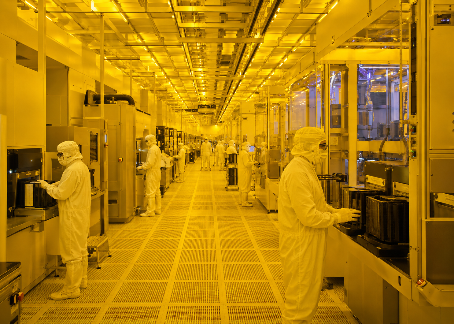
Semiconductor fabrication operates at sub-micron feature sizes where particle contamination measured in nanometres can cause defects. Freight that passes through standard warehouse environments or is handled without contamination control introduces contamination risk. For the most sensitive shipments — process chemicals, wafers, reticles — packaging integrity and handling environment matter enormously.
Export control compliance
Many semiconductor materials, components, and especially fabrication equipment are subject to export controls under the Export Administration Regulations (EAR) and in some cases ITAR. The movement of controlled semiconductor technology — particularly advanced lithography equipment, certain process tools, and high-end chips themselves — requires careful export licence management. A freight broker moving semiconductor equipment internationally needs to understand these requirements rather than treating them as someone else's problem.
Mode selection for semiconductor freight
- Next flight out (NFO): For line-down emergencies where the part is more than 500 miles away and the deadline is measured in hours. Your component travels on the next available commercial flight, with airport-capable couriers at both ends. See our NFO freight guide for detail on how this works.
- Dedicated ground: For distances under 500 miles, a dedicated vehicle dispatched immediately is typically faster door-to-door than NFO freight once airport processing time is included. No check-in window, no terminal handling — direct from supplier to fab gate.
- Hot shot: For smaller parts or samples moving regionally at high urgency. Immediate dispatch, dedicated vehicle, zero consolidation delay.
- Temperature-controlled dedicated: For process chemicals, biological materials, or temperature-sensitive components where the carrier vehicle needs active or passive temperature management throughout the move.
What to look for in a semiconductor freight broker
- 24/7 live dispatch — fab emergencies happen at 2am on Sundays
- Understanding of ESD handling requirements and ability to brief carriers
- Hazmat certification for process chemicals and specialty gas movements
- Experience with wafer and reticle packaging and handling requirements
- NFO capability at both origin and destination airports
- EAR/ITAR awareness for movements involving controlled technology
- Nationwide carrier network for immediate dispatch regardless of origin
KLAM Expeditors — semiconductor and technology freight
KLAM Expeditors is a licensed freight broker (MC# 1664023) providing expedited freight for semiconductor manufacturers, equipment suppliers, and technology companies across the United States. We offer 24/7 dispatch for line-down emergencies and time-critical semiconductor logistics, with a carrier network covering all 48 contiguous states and NFO capability at major US airports.
For semiconductor freight enquiries, call us directly at +1 510 331 6699. For related reading, see our guides on expedited freight for manufacturing plants and next flight out freight.